

- жЦдьГЇЩЬЃКTIЃЈЕТжнвЧЦїЃЌTexas InstrumentsЃЉ
- ВњЦЗРрБ№ЃКЪ§ОнзЊЛЛЦї
- ММЪѕРрФПЃКФЃЪ§зЊЛЛЦї (ADC) - ИпЫйФЃЪ§зЊЛЛЦї (>10MSPS)
- ЙІФмУшЪіЃК12 ЮЛЁЂ170MSPSЁЂ1.1GHz ЪфШыДјПэФЃЪ§зЊЛЛЦї (ADC)
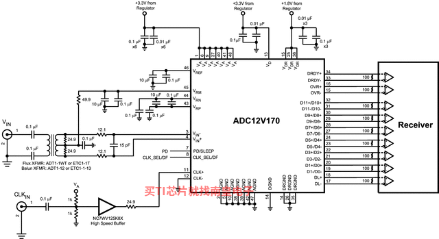
- ЕуЛїетРяДђПЊМАЯТдиADC12V170ЕФММЪѕЮФЕЕзЪСЯ
- TIДњРэЧўЕРЃЌЬсЙЉЕБШеЗЂЛѕЁЂбЯИёЕФжЪСПБъзМЃЌТњзуФњЕФФПБъМлИё

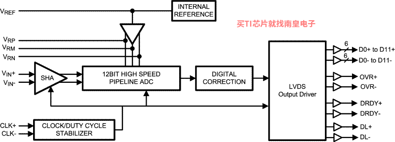
The ADC12V170 is a high-performance CMOS analog-to-digital converter with LVDS outputs. It is capable of converting analog input signals into 12-Bit digital words at rates up to 170 Mega Samples Per Second (MSPS). Data leaves the chip in a DDR (Dual Data Rate) format; this allows both edges of the output clock to be utilized while achieving a smaller package size. This converter uses a differential, pipelined architecture with digital error correction and an on-chip sample-and-hold circuit to minimize power consumption and the external component count, while providing excellent dynamic performance. A unique sample-and-hold stage yields a full-power bandwidth of 1.1 GHz. The ADC12V170 operates from dual +3.3V and +1.8V power supplies and consumes 781 mW of power at 170 MSPS.
The separate +1.8V supply for the digital output interface allows lower power operation with reduced noise. A power-down feature reduces the power consumption to 15 mW while still allowing fast wake-up time to full operation. In addition there is a sleep feature which consumes 50 mW of power and has a faster wake-up time.
The differential inputs provide a full scale differential input swing equal to 2 times the reference voltage. A stable 1.0V internal voltage reference is provided, or the ADC12V170 can be operated with an external reference.
Clock mode (differential versus single-ended) and output data format (offset binary versus 2's complement) are pin-selectable. A duty cycle stabilizer maintains performance over a wide range of input clock duty cycles.
The ADC12V170 is pin-compatible with the ADC14V155. It is available in a 48-lead WQFN package and operates over the industrial temperature range of −40°C to +85°C.
- 1.1 GHz Full Power Bandwidth
- Internal Sample-and-Hold Circuit
- Internal Precision 1.0V Reference
- Single-Ended or Differential Clock Modes
- Clock Duty Cycle Stabilizer
- Dual +3.3V and +1.8V Supply Operation
- Power-Down and Sleep Modes
- Offset Binary or 2's Complement Output Data Format
- LVDS Outputs
- Pin-Compatible: ADC14V155
- 48-Pin WQFN Package, (7x7x0.8mm, 0.5mm Pin-Pitch)
- Resolution: 12 Bits
- Conversion Rate: 170 MSPS
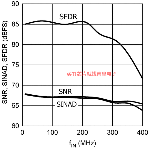
- SNR (fIN = 70 MHz): 67.2 dBFS (Typ)
- SFDR (fIN = 70 MHz): 85.8 dBFS (Typ)
- ENOB (fIN = 70 MHz): 10.9 Bits (Typ)
- Full Power Bandwidth: 1.1 GHZ (Typ)
- Power Consumption: 781 mW (Typ)
All trademarks are the property of their respective owners.
- Sample rate (Max) (MSPS)
- 170
- Resolution (Bits)
- 12
- Number of input channels
- 1
- Interface type
- DDR LVDS, Parallel LVDS
- Analog input BW (MHz)
- 1100
- Features
- Low Power
- Rating
- Catalog
- Input range (Vp-p)
- 2
- Power consumption (Typ) (mW)
- 781
- Architecture
- Pipeline
- SNR (dB)
- 67.9
- ENOB (Bits)
- 11
- SFDR (dB)
- 85.8
- Operating temperature range (C)
- -40 to 85
- Input buffer
- No
ADC12V170ЕФЭъећаЭКХгаЃКADC12V170CISQ/NOPBЃЌвдЯТЪЧетаЉВњЦЗЕФЙиМќВЮЪ§МАЙйЭјВЩЙКБЈМлЃК
ADC12V170CISQ/NOPBЃЌЙЄзїЮТЖШЃК-40 to 85ЃЌЗтзАЃКWQFN (RHS)-48ЃЌАќзАЪ§СПMPQЃК250ИіЃЌMSL ЕШМЖ/ЛиСїКИЗхжЕЮТЖШЃКLevel-3-260C-168 HRЃЌв§НХЖЦВу/КИЧђВФСЯЃКSNЃЌTIЙйЭјADC12V170CISQ/NOPBЕФХњСПUSDМлИёЃК33.541ЃЈ1000+ЃЉ

PSPICE-FOR-TI ЪЪгУгк TI ЩшМЦКЭФЃФтЙЄОпЕФ PSpice
PSpice for TI ПЩЬсЙЉАяжњЦРЙРФЃФтЕчТЗЙІФмЕФЩшМЦКЭЗТецЛЗОГЁЃДЫЙІФмЦыШЋЕФЩшМЦКЭЗТецЬзМўЪЙгУ Cadence ЕФФЃФтЗжЮів§ЧцЁЃPSpice for TI ПЩУтЗбЪЙгУЃЌАќРЈвЕФкГЌДѓЕФФЃаЭПтжЎвЛЃЌКИЧЮвУЧЕФФЃФтКЭЕчдДВњЦЗЯЕСавдМАОЋбЁЕФФЃФтааЮЊФЃаЭЁЃНшжњPSpice for TI ЕФЩшМЦКЭЗТецЛЗОГМАЦфФкжУЕФФЃаЭПтЃЌФњПЩЖдИДдгЕФЛьКЯаХКХЩшМЦНјааЗТецЁЃДДНЈЭъећЕФжеЖЫЩшБИЩшМЦКЭдаЭНтОіЗНАИЃЌШЛКѓдйНјааВМОжКЭжЦдьЃЌПЩЫѕЖЬВњЦЗЩЯЪаЪБМфВЂНЕЕЭПЊЗЂГЩБОЁЃ
дкPSpice for TI ЩшМЦКЭЗТецЙЄОпжаЃЌФњПЩвдЫбЫї TI (...)
- UC2832
- THS4215
- DAC7573
- UCC21540A
- TMP64-Q1
- LM2771
- LM95213
- SM320C6678-HIREL
- ADC3644
- LMX2541
- SN75158
- MSP430F47176
- MSP430F6779
- SN54LS697
- HDC3021-Q1
- BQ24312
- UCC1803
- DS92LV2422
- INA2134
- BQ2014H
- TPS22917DBVR
- COP8SDR9HLQ8
- TPS3125J12DBVT
- TL074CDG4
- MAX3243MDBREP
- DLPLCRC900EVM
- TRSF3232CPW
- LM5101SD/NOPB
- TPA005D12DCAR
- TPS92691QPWPTQ1
- TRSF3232IDBRG4
- TPS53119EVM-690
- SN74AHCT244NSR
- TAS2781EVM
- LM26LVCISDX-150/NOPB
- TPA2038D1YFFEVM
- MF10CCJ
- SN74HCT74DBR
- DS90LV012ATMF
- DS160PR410RGFTQ1
