
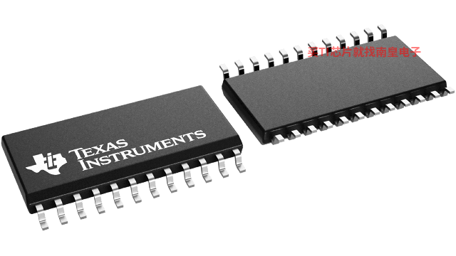
- 制造厂商:TI(德州仪器,Texas Instruments)
- 产品类别:开关与多路复用器
- 技术类目:模拟开关和多路复用器
- 功能描述:20V、8:1 差分、单通道模拟多路复用器
- 点击这里打开及下载CD4097B的技术文档资料
- TI代理渠道,提供当日发货、严格的质量标准,满足您的目标价格

CD4067B and CD4097B CMOS analog multiplexers/demultiplexers* are digitally controlled analog switches having low ON impedance, low OFF leakage current, and internal address decoding. In addition, the ON resistance is relatively constant over the full input-signal range. The CD4067B is a 16-channel multiplexer with four binary control inputs, A, B, C, D, and an inhibit input, arranged so that any combination of the inputs selects one switch.
The CD4097B is a differential 8-channel multiplexer having three binary control inputs, A, B, C, and an inhibit input. The inputs permit selection of one of eight pairs of switches.
A logic "1" present at the inhibit input turns all channels off.
The CD4067B and CD4097B types are supplied in 24-lead hermetic dual-in-line ceramic packages (F3A suffix), 24-lead dual-in-line plastic packages (E suffix), 24-lead small-outline packages (M, M96, and NSR suffixes), and 24-lead thin shrink small-outline packages (P and PWR suffixes).
- Low ON resistance: 125 (typ.) over 15 Vp-p signal-input range for VDD - VSS = 15 V
- High OFF resistance: channel leakage of ±10 pA (typ.) @ VDD - VSS = 10 V
- Matched switch characteristics: RON = 5 (typ.) for VDD - VSS = 15 V
- Very low quiescent power dissipation under all digital-control input and supply conditions: 0.2 uW (typ.) @ VDD - VSS = 10 V
- Binary address decoding on chip
- 5-V, 10-V, and 15-V parametric ratings
- 100% tested for quiescent current at 20 V
- Maximum input current of 1 A at 18 V over full package-temperature range; 100nA at 18 V and 25°C
- Meets all requirements of JEDEC Tentative Standard No. 13A, "Standard Specifications for Description of 'B' Series CMOS Devices"
- Applications:
- Analog and digital multiplexing and demultiplexing
- A/D and D/A conversion
- Siganl gating
* When these devices are used as demultiplexers, the channel in/out terminals are the outputs and the common out/in terminals are the inputs.
- Configuration
- 8:1
- Number of channels (#)
- 2
- Power supply voltage - single (V)
- 3.3, 5, 12, 16, 20
- Protocols
- Analog
- Ron (Typ) (Ohms)
- 125
- CON (Typ) (pF)
- 35
- Bandwidth (MHz)
- 20
- Operating temperature range (C)
- -55 to 125
- Features
- Break-before-make
- Input/output continuous current (Max) (mA)
- 10
- Rating
- Catalog
- Supply current (Typ) (uA)
- 0.04
CD4097B的完整型号有:CD4097BM、CD4097BPW、CD4097BPWR,以下是这些产品的关键参数及官网采购报价:
CD4097BM,工作温度:-55 to 125,封装:SOIC (DW)-24,包装数量MPQ:25个,MSL 等级/回流焊峰值温度:Level-1-260C-UNLIM,引脚镀层/焊球材料:NIPDAU,TI官网CD4097BM的批量USD价格:.154(1000+)
CD4097BPW,工作温度:-55 to 125,封装:TSSOP (PW)-24,包装数量MPQ:60个,MSL 等级/回流焊峰值温度:Level-1-260C-UNLIM,引脚镀层/焊球材料:NIPDAU,TI官网CD4097BPW的批量USD价格:.382(1000+)
CD4097BPWR,工作温度:-55 to 125,封装:TSSOP (PW)-24,包装数量MPQ:2000个,MSL 等级/回流焊峰值温度:Level-1-260C-UNLIM,引脚镀层/焊球材料:NIPDAU,TI官网CD4097BPWR的批量USD价格:.182(1000+)

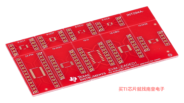
LEADED-ADAPTER1 用于快速测试 TI 5、8、10、16 和 24 引脚引线式封装的表面贴装转 DIP 接头适配器
EVM-LEADED1 板可对 TI 的常见引线式封装进行快速测试和电路板试验。该评估板具有足够的空间,可将 TI 的 D、DBQ、DCT、DCU、DDF、DGS、DGV 和 PW 表面贴装封装转换为 100mil DIP 接头。

- TPS60210
- TPS53632G
- LP2998-Q1
- TMS320F28378D
- LMH0387
- TPSM82866A
- DRV8703D-Q1
- TM4C1237H6PZ
- TPS715A
- LMH6654
- CD4098B
- DAC8218
- ADS5240
- DRV421
- SN74ACT373-EP
- LM293-N
- LM12H458
- TWL1103T-Q1
- OPA604
- DM3725
- SN74ALVCH16821DL
- TPS3808G15DRVR
- LM4892LDX
- TMAG5131C7DQDBZRQ1
- TCAN1051GVDQ1
- TL16C550DIPFB
- TPS74401RGRR
- RDK-ACIM
- OPA857IRGTT
- TLV320AIC27CPFB
- SN74LS74ADBR
- TPS51100DGQG4
- UC3705TG3
- DS90CR285MTDX/NOPB
- CC1201RHBR
- SN74AUP1G98YFPR
- LMP8271MAX/NOPB
- TLV3704IPWRG4
- ADS5242IPAP
- TPS40040DRBT
