

- 制造厂商:TI(德州仪器,Texas Instruments)
- 产品类别:时钟和计时
- 技术类目:时钟发生器
- 功能描述:具有 2.5V 或 3.3V LVCMOS 输出的可编程 4-PLL VCXO 时钟合成器
- 点击这里打开及下载CDCE949的技术文档资料
- TI代理渠道,提供当日发货、严格的质量标准,满足您的目标价格

The CDCE949 and CDCEL949 are modular PLL-based low cost, high-performance, programmable clock synthesizers, multipliers and dividers. They generate up to 9 output clocks from a single input frequency. Each output can be programmed in-system for any clock frequency up to 230 MHz, using up to four independent configurable PLLs.
The CDCEx949 has separate output supply pins, VDDOUT, 1.8 V for the CDCEL949, and 2.5 V to 3.3 V for CDCE949.
The input accepts an external crystal or LVCMOS clock signal. If an external crystal is used, an on-chip load capacitor is adequate for most applications. The value of the load capacitor is programmable from 0 to 20 pF. Additionally, an on-chip VCXO is selectable, allowing synchronization of the output frequency to an external control signal, that is, a PWM signal.
The deep M/N divider ratio allows the generation of zero-ppm audio or video, networking (WLAN, BlueTooth™, Ethernet, GPS) or Interface (USB, IEEE1394, Memory Stick) clocks from a reference input frequency, such as 27 MHz.
All PLLs support SSC (Spread-Spectrum Clocking). SSC can be Center-Spread or Down-Spread clocking. This is a common technique to reduce electro-magnetic interference (EMI).
Based on the PLL frequency and the divider settings, the internal loop-filter components are automatically adjusted to achieve high stability, and to optimize the jitter-transfer characteristics of each PLL.
The device supports non-volatile EEPROM programming for easy customization of the device to the application. It is preset to a factory-default configuration. It can be reprogrammed to a different application configuration before PCB assembly, or reprogrammed by in-system programming. All device settings are programmable through the SDA and SCL bus, a 2-wire serial interface.
Three programmable control inputs, S0, S1 and S2, can be used to control various aspects of operation including frequency selection, changing the SSC parameters to lower EMI, PLL bypass, power down, and choosing between low level or 3-state for the output-disable function.
The CDCEx949 operates in a 1.8-V environment. It operates within a temperature range of –40°C to 85°C.
- Member of Programmable Clock Generator Family
- CDCEx913: 1 PLLs, 3 Outputs
- CDCEx925: 2 PLLs, 5 Outputs
- CDCEx937: 3 PLLs, 7 Outputs
- CDCEx949: 4 PLLs, 9 Outputs
- In-System Programmability and EEPROM
- Serial Programmable Volatile Register
- Nonvolatile EEPROM to Store Customer Settings
- Flexible Input Clocking Concept
- External Crystal: 8 to 32 MHz
- On-Chip VCXO: Pull-Range ±150 ppm
- Single-Ended LVCMOS Up to 160MHz
- Free Selectable Output Frequency Up to 230MHz
- Low-Noise PLL Core
- PLL Loop Filter Components Integrated
- Low Period Jitter (Typical 60 ps)
- Separate Output Supply Pins
- CDCE949: 3.3 V and 2.5 V
- CDCEL949: 1.8 V
- Flexible Clock Driver
- Three User-Definable Control Inputs [S0/S1/S2], for Example, SSC Selection, Frequency Switching, Output Enable or Power Down
- Generates Highly Accurate Clocks for Video, Audio, USB, IEEE1394, RFID, Bluetooth, WLAN, Ethernet, and GPS
- Generates Common Clock Frequencies Used With TI-DaVinci, OMAP, DSPs
- Programmable SSC Modulation
- Enables 0-PPM Clock Generation
- 1.8-V Device Core Supply
- Wide Temperature Range: 40°C to 85°C
- Packaged in TSSOP
- Development and Programming Kit for Easy PLL Design and Programming (TI Pro-Clock)
- Function
- Clock synthesizer
- Number of outputs
- 9
- Output frequency (Max) (MHz)
- 230
- Core supply voltage (V)
- 1.8
- Output supply voltage (V)
- 2.5, 3.3
- Input type
- XTAL, LVCMOS
- Output type
- LVCMOS
- Operating temperature range (C)
- -40 to 85
- Features
- Integrated EEPROM, Multiplier or divider, Spread-spectrum clocking (SSC)
- Rating
- Catalog
CDCE949的完整型号有:CDCE949PW、CDCE949PWR,以下是这些产品的关键参数及官网采购报价:
CDCE949PW,工作温度:-40 to 85,封装:TSSOP (PW)-24,包装数量MPQ:60个,MSL 等级/回流焊峰值温度:Level-1-260C-UNLIM,引脚镀层/焊球材料:NIPDAU,TI官网CDCE949PW的批量USD价格:2.482(1000+)
CDCE949PWR,工作温度:-40 to 85,封装:TSSOP (PW)-24,包装数量MPQ:2000个,MSL 等级/回流焊峰值温度:Level-1-260C-UNLIM,引脚镀层/焊球材料:NIPDAU,TI官网CDCE949PWR的批量USD价格:2.068(1000+)

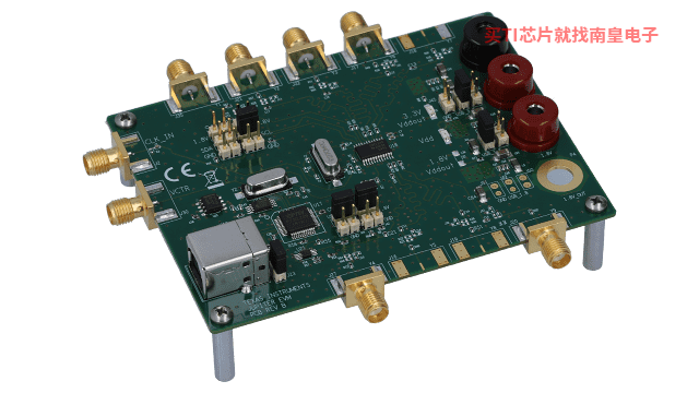
CDCE949PERF-EVM CDCE949 性能评估模块
The CDCE949Perf-Evaluation Module will help to verify the functionality and performance of CDCE949 with the options of crystal and 1.8V LVCMOS inputs. The outputs can be connected to the Oscilloscope directly with SMA cables. The below information/items can be included The EVM use’s (...)
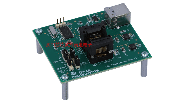
CDCEL9XXPROGEVM CDCE(L)949 系列 EEPROM 编程板
CDCE(L)949 系列时钟发生器集成了 EEPROM,允许在启动后保存默认频率设置。CDCEL9XXPROGEVM 是允许对原型样片或小批量生产进行快速编程的编程板。它适用于该系列的全部 8 款器件:CDCE949、CDCE937、CDCE925、CDCE913、CDCEL949、CDCEL937、CDCEL925 和 CDCEL913,并且带有易于使用的通用插座。
此外还提供另一个用于性能测试和评估的 EVM,其器件型号为 CDCE(L)9xxPERF-EVM,此性能评估模块适用于每个单独器件。
Drivers for the CDCEL9xx programmer EVM
TI's ClockPro software allows users to program/configure the following devices in a friendly GUI interface:- CDCE949
- CDCE937
- CDCE925
- CDCE913
- CDCE906
- CDCE706
- CDCEL949
- CDCEL937
- CDCEL925
- CDCEL913
It is intended to be used with the evaluation modules of the above devices.
ClockPro Software (Rev. E)
PSpice for TI 可提供帮助评估模拟电路功能的设计和仿真环境。此功能齐全的设计和仿真套件使用 Cadence 的模拟分析引擎。PSpice for TI 可免费使用,包括业内超大的模型库之一,涵盖我们的模拟和电源产品系列以及精选的模拟行为模型。借助PSpice for TI 的设计和仿真环境及其内置的模型库,您可对复杂的混合信号设计进行仿真。创建完整的终端设备设计和原型解决方案,然后再进行布局和制造,可缩短产品上市时间并降低开发成本。
在PSpice for TI 设计和仿真工具中,您可以搜索 TI (...)
CLOCK-TREE-ARCHITECT 时钟树架构编程软件
时钟树架构是一款时钟树综合工具,可根据您的系统要求生成时钟树解决方案,从而帮助您简化设计流程。该工具从庞大的时钟产品数据库中提取数据,然后生成系统级多芯片时钟解决方案。TIDA-010057 Ultrasound smart probe power supply reference design
医疗成像领域的巨大技术进步和高集成度,特别是手持式超声波智能探头的出现,促使工程师开发出高效率、抗噪声的小尺寸电源解决方案。此参考设计阐述了端到端电源和数据解决方案,适用于我们采用 TX7332 发送芯片和 AFE5832LP 接收芯片的高性能 128 通道 Tx/64 通道 Rx 超声波智能探头。通过 5V USB Type-C™ 输入,电源树可生成用于发送的单级无变压器高压(高达 +/-80V,并且高度小于 5mm)以及用于 AFE 和 FPGA 的负载点低压。此设计可实现低噪声(纹波电压小于 10mV)高效电源轨并提高热性能(温升小于 (...)

- TMS320F28232-Q1
- ADS131M08
- TPS61325
- ADS6142-HT
- TPS7H5006-SEP
- LM2758
- TL1451A-EP
- TPS24770
- TPA6136A2
- MSP430F5524
- SN54HC273
- CD74HC4514
- DAC5687
- TLC081
- CD54HCT564
- SN74LVC74A
- MSP430F5171
- TPS54560B-Q1
- BQ24140
- TPS54615-EP
- LP3981ILD-2.8/NOPB
- LMV761MFX
- LM4820ITP-6/NOPB
- TL3016IPWRG4
- 66AK2H12DAAW24
- INA117BM-3
- THS4150IDGKRG4
- ULN2003ANE4
- MM74HC191N
- UCC2585D
- PCM1821IRTER
- TLV707115DQNT
- LP3981IMMX-3.0
- CAHCT1G126QDCKRG4
- TRSF3223EIRGWR
- THS3125CDR
- TLIN1029ADRQ1
- UCC28702DBVR
- TPS60204DGSR
- MSP430F5419AIZQWT
