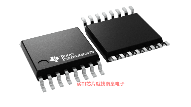
- 制造厂商:TI
- 产品类别:时钟和计时
- 技术类目:时钟缓冲器
- 功能描述:具有 8 路输出的 3.3V x4 时钟倍频器
- 点击这里打开及下载CDCVF25084的技术文档资料
- TI代理渠道,提供当日发货、严格的质量标准,满足您的目标价格

The CDCVF25084 is a high-performance, low-skew, low-jitter, phase-lock loop clock multiplier. It uses a PLL to precisely align, in both frequency and phase, the output clocks to the input clock signal including a multiplication factor of four. The CDCVF25084 operates from a nominal supply voltage of 3.3 V. The device also includes integrated series-damping resistors in the output drivers that make it ideal for driving point-to-point loads.
Two banks of four outputs each provide low-skew, low-jitter copies of CLKIN x four. All outputs operate at the same frequency. Output duty cycles are adjusted to 50%, independent of duty cycle at CLKIN. The device automatically goes into power-down mode when no input signal is applied to CLKIN and the outputs go into a low state. Unlike many products containing PLLs, the CDCVF25084 does not require an external RC network. The loop filter for the PLL is included on-chip, minimizing component count, space, and cost.
Because it is based on a PLL circuitry, the CDCVF25084 requires a stabilization time to achieve phase lock of the feedback signal to the reference signal. This stabilization is required following power up and application of a fixed-frequency signal at CLKIN and any following changes to the PLL reference.
The CDCVF25084 is characterized for operation from –40°C to 85°C.
- Phase-Locked Loop-Based Multiplier by Four
- Input Frequency Range: 2.5 MHz to 45 MHz
- Output Frequency Range: 10 MHz to 180 MHz
- LVCMOS/LVTT I/O Compatible
- Low Jitter (Cycle-Cycle): ±120 ps Over the Range 75 MHz to 180 MHz
- Distributes One Clock Input to Two Banks of Four Outputs
- Auto Frequency Detection to Disable Device (Power-Down Mode)
- Operates From Single 3.3-V Supply
- Industrial Temperature Range 40°C to 85°C
- 25- On-Chip Series Damping Resistors
- No External RC Network Required
- Spread Spectrum Clock Compatible (SSC)
- Available in 16-Pin TSSOP Package
- Function
- Zero-delay
- Additive RMS jitter (Typ) (fs)
- 120
- Output frequency (Max) (MHz)
- 180
- Number of outputs
- 8
- Output supply voltage (V)
- 3.3
- Core supply voltage (V)
- 3.3
- Output skew (ps)
- 150
- Features
- Spread spectrum clocking (SSC)
- Operating temperature range (C)
- -40 to 85
- Rating
- Catalog
- Output type
- LVTTL
- Input type
- LVTTL
CDCVF25084的完整型号有:CDCVF25084PW、CDCVF25084PWR,以下是这些产品的关键参数及官网采购报价:
CDCVF25084PW,工作温度:-40 to 85,封装:TSSOP (PW)-16,包装数量MPQ:90个,MSL 等级/回流焊峰值温度:Level-1-260C-UNLIM,引脚镀层/焊球材料:NIPDAU,TI官网CDCVF25084PW的批量USD价格:4.685(1000+)
CDCVF25084PWR,工作温度:-40 to 85,封装:TSSOP (PW)-16,包装数量MPQ:2000个,MSL 等级/回流焊峰值温度:Level-1-260C-UNLIM,引脚镀层/焊球材料:NIPDAU,TI官网CDCVF25084PWR的批量USD价格:3.964(1000+)

CDCVF25084 IBIS Model
PSpice for TI 可提供帮助评估模拟电路功能的设计和仿真环境。此功能齐全的设计和仿真套件使用 Cadence 的模拟分析引擎。PSpice for TI 可免费使用,包括业内超大的模型库之一,涵盖我们的模拟和电源产品系列以及精选的模拟行为模型。借助PSpice for TI 的设计和仿真环境及其内置的模型库,您可对复杂的混合信号设计进行仿真。创建完整的终端设备设计和原型解决方案,然后再进行布局和制造,可缩短产品上市时间并降低开发成本。
在PSpice for TI 设计和仿真工具中,您可以搜索 TI (...)


