
- 制造厂商:TI(德州仪器,Texas Instruments)
- 产品类别:接口
- 技术类目:LVDS、M-LVDS 和 PECL IC
- 功能描述:单路全双工 LVDS 收发器
- 点击这里打开及下载SN65LVDS180的技术文档资料
- TI代理渠道,提供当日发货、严格的质量标准,满足您的目标价格

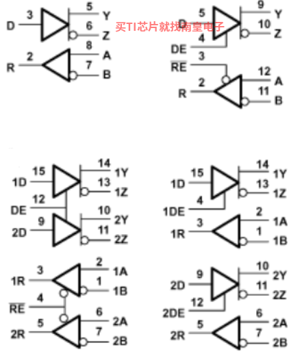
The SN65LVDS179, SN65LVDS180, SN65LVDS050, and SN65LVDS051 devices are differential line drivers and receivers that use low-voltage differential signaling (LVDS) to achieve signaling rates as high as 400 Mbps. The TIA/EIA-644 standard-compliant electrical interface provides a minimum differential output voltage magnitude of 247 mV into a 100-Ω load and receipt of 100-mV signals with up to 1 V of ground potential difference between a transmitter and receiver.
These devices offer various driver, receiver, and enabling combinations in industry-standard footprints. Because these devices are intended for use in simplex or distributed simplex bus structures, the driver enable function does not put the differential outputs into a high-impedance state but rather disconnects the input and reduces the quiescent power used by the device. For these functions with a high-impedance driver output, see the SN65LVDM series of devices. All devices are characterized for operation from –40°C to 85°C.
- Meets or Exceeds the Requirements of ANSI TIA/EIA-644-1995 Standard
- Full-Duplex Signaling Rates up to 150 Mbps
- Bus-Pin ESD Exceeds 12 kV
- Operates From a Single 3.3-V Supply
- Low-Voltage Differential Signaling With Typical Output Voltages of 350 mV and a 100-Ω Load
- Propagation Delay Times
- Driver: 1.7 ns Typical
- Receiver: 3.7 ns Typical
- Power Dissipation at 200 MHz
- Driver: 25 mW Typical
- Receiver: 60 mW Typical
- LVTTL Input Levels Are 5-V Tolerant
- Receiver Maintains High Input Impedance With VCC < 1.5 V
- Receiver Has Open-Circuit Fail Safe
- Function
- Transceiver
- Protocols
- LVDS
- Number of transmitters
- 1
- Number of receivers
- 1
- Supply voltage (V)
- 3.3
- Signaling rate (Mbps)
- 400, 150
- Input signal
- LVDS, LVTTL
- Output signal
- LVDS, LVTTL
- Rating
- Catalog
- Operating temperature range (C)
- -40 to 85
SN65LVDS180的完整型号有:SN65LVDS180D、SN65LVDS180DR、SN65LVDS180PW、SN65LVDS180PWR,以下是这些产品的关键参数及官网采购报价:
SN65LVDS180D,工作温度:-40 to 85,封装:SOIC (D)-14,包装数量MPQ:50个,MSL 等级/回流焊峰值温度:Level-1-260C-UNLIM,引脚镀层/焊球材料:NIPDAU,TI官网SN65LVDS180D的批量USD价格:1.665(1000+)
SN65LVDS180DR,工作温度:-40 to 85,封装:SOIC (D)-14,包装数量MPQ:2500个,MSL 等级/回流焊峰值温度:Level-1-260C-UNLIM,引脚镀层/焊球材料:NIPDAU,TI官网SN65LVDS180DR的批量USD价格:1.435(1000+)
SN65LVDS180PW,工作温度:-40 to 85,封装:TSSOP (PW)-14,包装数量MPQ:90个,MSL 等级/回流焊峰值温度:Level-1-260C-UNLIM,引脚镀层/焊球材料:NIPDAU,TI官网SN65LVDS180PW的批量USD价格:1.665(1000+)
SN65LVDS180PWR,工作温度:-40 to 85,封装:TSSOP (PW)-14,包装数量MPQ:2000个,MSL 等级/回流焊峰值温度:Level-1-260C-UNLIM,引脚镀层/焊球材料:NIPDAU,TI官网SN65LVDS180PWR的批量USD价格:1.435(1000+)

SN65LVDS180 IBIS Model
PSpice for TI 可提供帮助评估模拟电路功能的设计和仿真环境。此功能齐全的设计和仿真套件使用 Cadence 的模拟分析引擎。PSpice for TI 可免费使用,包括业内超大的模型库之一,涵盖我们的模拟和电源产品系列以及精选的模拟行为模型。借助PSpice for TI 的设计和仿真环境及其内置的模型库,您可对复杂的混合信号设计进行仿真。创建完整的终端设备设计和原型解决方案,然后再进行布局和制造,可缩短产品上市时间并降低开发成本。
在PSpice for TI 设计和仿真工具中,您可以搜索 TI (...)
TINA-TI 基于 SPICE 的模拟仿真程序
TINA-TI 提供了 SPICE 所有的传统直流、瞬态和频域分析以及更多。TINA 具有广泛的后处理功能,允许您按照希望的方式设置结果的格式。虚拟仪器允许您选择输入波形、探针电路节点电压和波形。TINA 的原理图捕获非常直观 - 真正的“快速入门”。TINA-TI 安装需要大约 500MB。直接安装,如果想卸载也很容易。我们相信您肯定会爱不释手。
TINA 是德州仪器 (TI) 专有的 DesignSoft 产品。该免费版本具有完整的功能,但不支持完整版 TINA 所提供的某些其他功能。
如需获取可用 TINA-TI 模型的完整列表,请参阅:SpiceRack - 完整列表
需要 HSpice (...)


- CSD18542KTT
- UCC21739-Q1
- TPS65219
- TPS65023B
- DS92LV3242
- SN65LVDS100
- TMS320F280041C
- ADS1284
- TLC1518
- TS3USB3031
- LM2704
- CD74ACT04
- TPS536C9
- DAC7725
- AMC3336
- TPS62304
- SN74LV4053A
- SN74CB3Q3253
- TS3L301
- OPA170-Q1
- BQ2002FSN
- LM135AH/NOPB
- PT7771N
- SN74ABT8952DL
- DAC7801LP
- TLC0820ACDWR
- TRS3222IDW
- TMS320C6457CGMHA2
- PCM1760U-X
- LM3S608-EGZ50-C2T
- SN74ALS648-1NT
- CD40174BEE4
- PCM1861QDBTRQ1
- SN74AHC74PWRG4
- TB3R2D
- SN74LVTH245ADW
- CD74HCT40103M96
- LP5550SQX/NOPB
- DRV8421ADGQR
- AMC1303M2510DWVR
