

- 制造厂商:TI(德州仪器,Texas Instruments)
- 产品类别:接口
- 技术类目:其他接口
- 功能描述:FlatLink 接收器
- 点击这里打开及下载SN75LVDS82的技术文档资料
- TI代理渠道,提供当日发货、严格的质量标准,满足您的目标价格

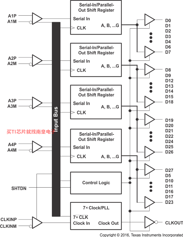
The SN75LVDS82 FlatLink™ receiver contains four serial-in, 7-bit parallel-out shift registers, a 7× clock synthesizer, and five low-voltage differential signaling (LVDS) line receivers in a single integrated circuit.
These functions allow receipt of synchronous data from a compatible transmitter, such as the SN75LVDS83B, over five balanced-pair conductors, and expansion to 28 bits of single-ended low-voltage TTL (LVTTL) synchronous data at a lower transfer rate. The SN75LVDS82 can also be used with the SN75LVDS84 for 21-bit transfers.
When receiving, the high-speed LVDS data is received and loaded into registers at the rate of seven times (7×) the LVDS input clock (CLKIN). The data is then unloaded to a 28-bit-wide LVTTL parallel bus at the CLKIN rate. A phase-locked loop (PLL) clock synthesizer circuit generates a 7× clock for internal clocking and an output clock for the expanded data. The SN75LVDS82 presents valid data on the falling edge of the output clock (CLKOUT).
The SN75LVDS82 requires only five line-termination resistors for the differential inputs and little or no control. The data bus appears the same at the input to the transmitter and output of the receiver with the data transmission transparent to the user.
The only possible user intervention is the use of the shutdown/clear (SHTDN) active-low input to inhibit the clock and shut off the LVDS receivers for lower power consumption. A low-level on SHTDN clears all internal registers to a low level and places the TTL outputs in a high-impedance state.
The SN75LVDS82 is characterized for operation over ambient air temperatures of 0°C to 70°C.
- 4:28 Data Channel Expansion at up to 1904 MbpsThroughput
- Suited for SVGA, XGA, or SXGA Display Data Transmission From Controller to Display With Very Low EMI
- Four Data Channels and Clock Low-Voltage Differential Channels In and 28 Data and Clock Low-Voltage TTL Channels Out
- Operates From a Single 3.3-V Supply With 250 mW (Typical)
- 5-V Tolerant SHTDN Input
- Falling Clock-Edge-Triggered Outputs
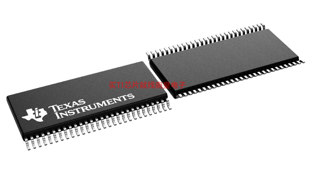
- Packaged in Thin Shrink Small-Outline Package (TSSOP) With 20-Mil Terminal Pitch
- Consumes Less Than 1 mW When Disabled
- Pixel Clock Frequency Range of 31 MHz to 68 MHz
- No External Components Required for PLL
- Inputs Meet or Exceed the Requirements of ANSI EIA/TIA-644 Standard
- Operating temperature range (C)
- 0 to 70
SN75LVDS82的完整型号有:SN75LVDS82DGG、SN75LVDS82DGGR,以下是这些产品的关键参数及官网采购报价:
SN75LVDS82DGG,工作温度:0 to 70,封装:TSSOP (DGG)-56,包装数量MPQ:35个,MSL 等级/回流焊峰值温度:Level-2-260C-1 YEAR,引脚镀层/焊球材料:NIPDAU,TI官网SN75LVDS82DGG的批量USD价格:2.5(1000+)
SN75LVDS82DGGR,工作温度:0 to 70,封装:TSSOP (DGG)-56,包装数量MPQ:2000个,MSL 等级/回流焊峰值温度:Level-2-260C-1 YEAR,引脚镀层/焊球材料:NIPDAU,TI官网SN75LVDS82DGGR的批量USD价格:2.1(1000+)

SN75LVDS82 IBIS Model
PSpice for TI 可提供帮助评估模拟电路功能的设计和仿真环境。此功能齐全的设计和仿真套件使用 Cadence 的模拟分析引擎。PSpice for TI 可免费使用,包括业内超大的模型库之一,涵盖我们的模拟和电源产品系列以及精选的模拟行为模型。借助PSpice for TI 的设计和仿真环境及其内置的模型库,您可对复杂的混合信号设计进行仿真。创建完整的终端设备设计和原型解决方案,然后再进行布局和制造,可缩短产品上市时间并降低开发成本。
在PSpice for TI 设计和仿真工具中,您可以搜索 TI (...)
TINA-TI 基于 SPICE 的模拟仿真程序
TINA-TI 提供了 SPICE 所有的传统直流、瞬态和频域分析以及更多。TINA 具有广泛的后处理功能,允许您按照希望的方式设置结果的格式。虚拟仪器允许您选择输入波形、探针电路节点电压和波形。TINA 的原理图捕获非常直观 - 真正的“快速入门”。TINA-TI 安装需要大约 500MB。直接安装,如果想卸载也很容易。我们相信您肯定会爱不释手。
TINA 是德州仪器 (TI) 专有的 DesignSoft 产品。该免费版本具有完整的功能,但不支持完整版 TINA 所提供的某些其他功能。
如需获取可用 TINA-TI 模型的完整列表,请参阅:SpiceRack - 完整列表
需要 HSpice (...)
- MAX3318
- UCC27611
- TS5A3159-EP
- TPS51650
- TL052
- TLV320AIC3256
- TLV2624
- REF70
- ISO1432
- SN54AS652
- SN74HC74-EP
- TPS80032
- UCC2580-1
- TPS2069D
- TPS2032-Q1
- LM51561
- THS4520-DIE
- SN65HVD485E
- TPS76901-HT
- SN74ABT162244
- DSD1792ADBG4
- TPS65642AYFFR
- TLV2197QDGKRQ1
- TPS54311PWP
- LM20145MHX/NOPB
- TPS61182RTERG4
- UCC37325P
- CDCV304PWG4
- SN74LVC244ARKSR
- 5962-89845022A
- UCC27201ATDA2
- LM3S2U93-IBZ80-A2T
- SN74AHCT240QPWRQ1
- ONET1130ECRSMR
- TLV320AIC3212IYZFR
- TVP70025IPZP
- BQ29400PWR
- TPS3839K33DBZT
- LP5866RKPR
- SN74ACT3631-30PQ
