

- 制造厂商:TI(德州仪器,Texas Instruments)
- 产品类别:数据转换器
- 技术类目:模数转换器 (ADC) - 高速模数转换器 (>10MSPS)
- 功能描述:11 位、125MSPS、1.1GHz 输入带宽模数转换器 (ADC)
- 点击这里打开及下载ADC11C125的技术文档资料
- TI代理渠道,提供当日发货、严格的质量标准,满足您的目标价格

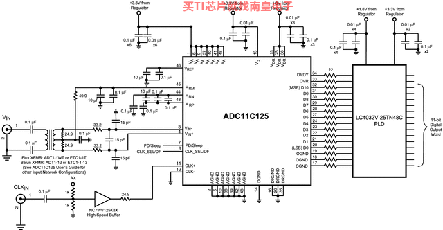
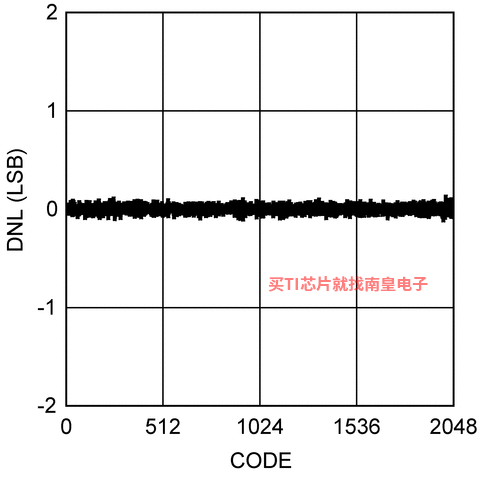
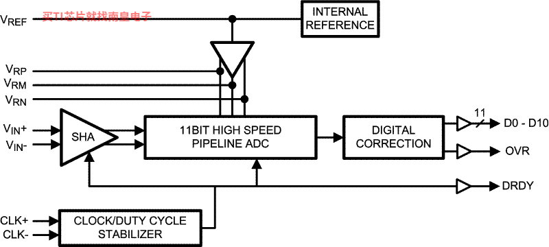
The ADC11C125 is a high-performance CMOS analog-to-digital converter capable of converting analog input signals into 11-Bit digital words at rates up to 125 Mega Samples Per Second (MSPS). This converter uses a differential, pipelined architecture with digital error correction and an on-chip sample-and-hold circuit to minimize power consumption and the external component count, while providing excellent dynamic performance. A unique sample-and-hold stage yields a full-power bandwidth of 1.1 GHz. The ADC11C125 operates from dual +3.3V and +1.8V power supplies and consumes 608 mW of power at 125 MSPS.
The separate +1.8V supply for the digital output interface allows lower power operation with reduced noise. A power-down feature reduces the power consumption to 5 mW while still allowing fast wake-up time to full operation. In addition there is a sleep feature which consumes 50 mW of power and has a faster wake-up time.
The differential inputs provide a full scale differential input swing equal to 2 times the reference voltage. A stable 1.0V internal voltage reference is provided, or the ADC11C125 can be operated with an external reference.
Clock mode (differential versus single-ended) and output data format (offset binary versus 2's complement) are pin-selectable. A duty cycle stabilizer maintains performance over a wide range of input clock duty cycles.
The ADC11C125 is pin compatible with the ADC12C170 and the ADC14155.
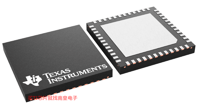
It is available in a 48-lead WQFN package and operates over the industrial temperature range of −40°C to +85°C.
- 1.1 GHz Full Power Bandwidth
- Internal Sample-and-Hold Circuit
- Low Power Consumption
- Internal Precision 1.0V Reference
- Single-Ended or Differential Clock Modes
- Clock Duty Cycle Stabilizer
- Dual +3.3V and +1.8V Supply Operation
- Power-Down and Sleep Modes
- Offset Binary or 2's Complement Output Data Format
- Pin-Compatible: ADC14155, ADC12C170, ADC11C170
- 48-pin WQFN Package, (7x7x0.8mm, 0.5mm Pin-Pitch)
- Resolution 11 Bits
- Conversion Rate 125 MSPS
- SNR (fIN = 70 MHz) 65.5 dBFS (typ)
- SFDR (fIN = 70 MHz) 88.2 dBFS (typ)
- ENOB (fIN = 70 MHz) 10.5 bits (typ)
- Full Power Bandwidth 1.1 GHz (typ)
- Power Consumption 608 mW (typ)
All trademarks are the property of their respective owners.
- Sample rate (Max) (MSPS)
- 125
- Resolution (Bits)
- 11
- Number of input channels
- 1
- Interface type
- Parallel CMOS
- Analog input BW (MHz)
- 1100
- Features
- Low Power
- Rating
- Catalog
- Input range (Vp-p)
- 2
- Power consumption (Typ) (mW)
- 608
- Architecture
- Pipeline
- SNR (dB)
- 65.7
- ENOB (Bits)
- 10.6
- SFDR (dB)
- 88.2
- Operating temperature range (C)
- -45 to 85
- Input buffer
- No
ADC11C125的完整型号有:ADC11C125CISQ/NOPB,以下是这些产品的关键参数及官网采购报价:
ADC11C125CISQ/NOPB,工作温度:-45 to 85,封装:WQFN (RHS)-48,包装数量MPQ:250个,MSL 等级/回流焊峰值温度:Level-3-260C-168 HR,引脚镀层/焊球材料:SN,TI官网ADC11C125CISQ/NOPB的批量USD价格:17.037(1000+)

PSPICE-FOR-TI 适用于 TI 设计和模拟工具的 PSpice
PSpice for TI 可提供帮助评估模拟电路功能的设计和仿真环境。此功能齐全的设计和仿真套件使用 Cadence 的模拟分析引擎。PSpice for TI 可免费使用,包括业内超大的模型库之一,涵盖我们的模拟和电源产品系列以及精选的模拟行为模型。借助PSpice for TI 的设计和仿真环境及其内置的模型库,您可对复杂的混合信号设计进行仿真。创建完整的终端设备设计和原型解决方案,然后再进行布局和制造,可缩短产品上市时间并降低开发成本。
在PSpice for TI 设计和仿真工具中,您可以搜索 TI (...)
- SN54AC245
- LM43603-Q1
- BQ24780S
- SN54HCT245
- ADC32RF54
- CDCL1810A
- LP3892
- TPS56121
- LM5145
- TLV2774-EP
- SN54AHCT573
- LMT89
- TPS62823
- CD54AC32
- TLV3491
- DS90C365A
- TLV2475
- SN74LVC1G32
- SN54LS194A
- CD74AC153
- LF411CD
- MSP432P411YTPZ
- SN74LV08APWRG3
- 9317CPC
- SN74ALVCF162835VR
- 74FCT374ASCX
- CD4527BNS
- TPS51113DRCT
- BQ29412PWR
- TP3404V/63SN
- LMV358QPWE4
- LP2981IM5-3.6
- BQ2003PN
- TPS65279DAP
- OPA4340UA/2K5
- OPA191IDBVT
- TPS3823-30DBVR
- 5962-89511012A
- SN0305042RTHR
- MSP430F67791IPZ
