
- 制造厂商:TI(德州仪器,Texas Instruments)
- 产品类别:逻辑和电压转换
- 技术类目:触发器、锁存器和寄存器 - 移位寄存器
- 功能描述:CMOS 4 级并行输入/并行输出移位寄存器
- 点击这里打开及下载CD4035B的技术文档资料
- TI代理渠道,提供当日发货、严格的质量标准,满足您的目标价格

CD4035B is a four-stage clocked signal serial register with provision for synchronous PARALLEL inputs to each stage and SERIAL inputs to the first stage via JK\ logic. Register stages 2, 3, and 4 are coupled in a serial D flip-flop configuration when the register is in the serial mode (PARALLEL/SERIAL control low).
Parallel entry into each register stage is permitted when the PARALLEL/SERIAL control is high.
In the parallel or serial mode information is transferred on positive clock transitions.
When the TRUE/COMPLEMENT control is high, the true contents of the register are available at the output terminals. When the TRUE/COMPLEMENT control is low, the outputs are the complements of the data in the register. THe TRUE/COMPLEMENT control functions asynchronously with respect to the CLOCK signal.
JK\ input logic is provided on the first stage SERIAL input to minimize logic requirements particularly in counting and sequence-generation applications. With JK\ inputs connected together, the first stage becomes a D flip-flop. An asynchronous common RESET is also provided.
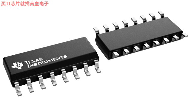
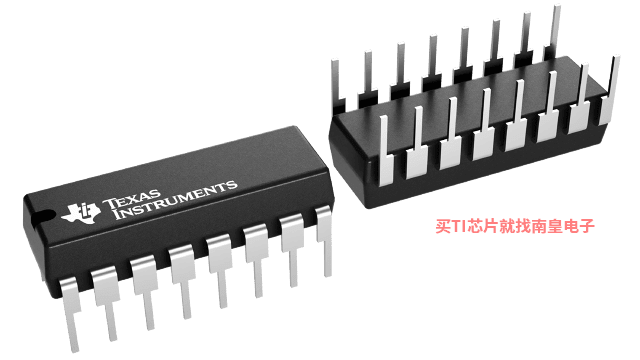
The CD4035B types are supplied in 16-lead hermetic dual-in-line ceramic packages (F3A suffix), 16-lead dual-in-line plastic packages (E suffix), 16-lead small-outline packages (M, M96, MT and NSR suffixes), and 16-lead thin shrink small-outline packages (PW and PWR suffixes).
- 4-Stage clocked shift operation
- Synchronous parallel entry on all 4 stages
- JK\ inputs on first stage
- Asynchronous True/Complement control on all outputs
- Static flip-flop operation; Master-slave configuration
- Buffered inputs and outputs
- High speed 12 MHz (typ.) at VDD = 10 V
- 100% tested for quiescent current at 20 V
- Standardized, symmetrical output characteristics
- 5-V, 10-V, and 15-V parametric ratings
- Meets all requirements of JEDEC Tentative Standard No. 13A, "Standard Specifications for Description of 'B' Series CMOS Devices"
- Applications:
- Counters, Registers
- Arithmetic-unit registers
- Shift-left shift right registers
- Serial-to-parallel/parallel-to-serial conversions
- Sequence generation
- Control circuits
- Code conversion
- Counters, Registers
- Configuration
- Universal
- Bits (#)
- 4
- Technology Family
- CD4000
- Supply voltage (Min) (V)
- 3
- Supply voltage (Max) (V)
- 18
- Input type
- Standard CMOS
- Output type
- Push-Pull
- Clock Frequency (MHz)
- 8.5
- IOL (Max) (mA)
- 4.2
- IOH (Max) (mA)
- -4.2
- ICC (Max) (uA)
- 3000
- Features
- Balanced outputs, Standard speed (tpd > 50ns), Positive input clamp diode
CD4035B的完整型号有:CD4035BE、CD4035BM、CD4035BM96、CD4035BPWR,以下是这些产品的关键参数及官网采购报价:
CD4035BE,工作温度:-55 to 125,封装:PDIP (N)-16,包装数量MPQ:25个,MSL 等级/回流焊峰值温度:N/A for Pkg Type,引脚镀层/焊球材料:NIPDAU,TI官网CD4035BE的批量USD价格:.481(1000+)
CD4035BM,工作温度:-55 to 125,封装:SOIC (D)-16,包装数量MPQ:40个,MSL 等级/回流焊峰值温度:Level-1-260C-UNLIM,引脚镀层/焊球材料:NIPDAU,TI官网CD4035BM的批量USD价格:.501(1000+)
CD4035BM96,工作温度:-55 to 125,封装:SOIC (D)-16,包装数量MPQ:2500个,MSL 等级/回流焊峰值温度:Level-1-260C-UNLIM,引脚镀层/焊球材料:NIPDAU,TI官网CD4035BM96的批量USD价格:.424(1000+)
CD4035BPWR,工作温度:-55 to 125,封装:TSSOP (PW)-16,包装数量MPQ:2000个,MSL 等级/回流焊峰值温度:Level-1-260C-UNLIM,引脚镀层/焊球材料:NIPDAU,TI官网CD4035BPWR的批量USD价格:.424(1000+)

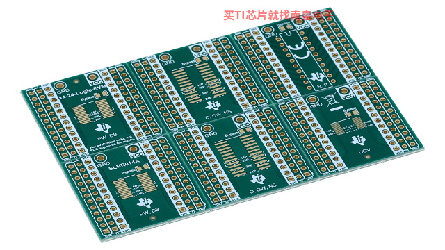
14-24-LOGIC-EVM 支持 14 到 24 引脚 PW、DB、D、DW、NS、DYY 和 DGV 封装的通用逻辑 EVM
该 EVM 设计用于支持采用 14 至 24 引脚 D、DW、DB、NS、PW、DYY 或 DGV 封装的任何逻辑器件。

- TPS62410-Q1
- SN54LS38
- TPS92830-Q1
- LMP8640
- TMAG5111-Q1
- ADS7853
- TPS563211
- ADS6445
- VSP5610
- SN54ALS30A
- TLE2061M
- CD4043B
- DS92LV18
- DAC7616
- TMUX1136
- TL031
- DS08MB200
- AMC23C12
- DAC8802
- TLV320AIC22C
- LM3671MFX-2.5/NOPB
- TPS54060QDGQRQ1
- SN74AC14PWRG4
- SN74HC08QPWRQ1
- BQ24800EVM
- AFE4460YBGT
- UC2825AQDWREPG4
- DAC8871SBPWR
- SN74HC540PWR
- TLV2462QDR
- LM3S2911-EQC50-A2
- LM3502ITL-35/NOPB
- SN74CBT3306CDR
- SN75452BPG4
- SN75471P
- LM1117DTX-5.0
- LM5168FDDAR
- LP8345CDTX-2.5/NOPB
- LM5009MMX/NOPB
- LM3S6753-EQC50-A2T
