

- 制造厂商:TI(德州仪器,Texas Instruments)
- 产品类别:时钟和计时
- 技术类目:时钟发生器
- 功能描述:具有 2.5V 或 3.3V LVCMOS 输出的可编程 2-PLL VCXO 时钟合成器
- 点击这里打开及下载CDCE925的技术文档资料
- TI代理渠道,提供当日发货、严格的质量标准,满足您的目标价格

The CDCE925 and CDCEL925 are modular PLL-based low-cost, high-performance, programmable clock synthesizers, multipliers, and dividers. They generate up to five output clocks from a single input frequency. Each output can be programmed in-system for any clock frequency up to 230 MHz, using up to two independent configurable PLLs.
The CDCEx925 has a separate output supply pin, VDDOUT, which is 1.8 V for CDCEL925 and 2.5 V to 3.3 V for CDCE925.
The input accepts an external crystal or LVCMOS clock signal. In case of a crystal input, an on-chip load capacitor is adequate for most applications. The value of the load capacitor is programmable from 0 to 20 pF. Additionally, an on-chip VCXO is selectable which allows synchronization of the output frequency to an external control signal, that is, PWM signal.
The deep M/N divider ratio allows the generation of zero-ppm audio/video, networking (WLAN, Bluetooth, Ethernet, GPS), or interface (USB, IEEE1394, memory stick) clocks from a 27-MHz reference input frequency, for example.
All PLLs support SSC (spread-spectrum clocking). SSC can be center-spread or down-spread clocking, which is a common technique to reduce electromagnetic interference (EMI).
Based on the PLL frequency and the divider settings, the internal loop filter components are automatically adjusted to achieve high stability and optimized jitter transfer characteristic of each PLL.
The device supports nonvolatile EEPROM programming for easy customization of the device in the application. It is preset to a factory default configuration and can be reprogrammed to a different application configuration before it goes onto the PCB or reprogrammed by in-system programming. All device settings are programmable through the SDA/SCL bus, a 2-wire serial interface.
Three, free programmable control inputs, S0, S1, and S2, can be used to select different frequencies, or change the SSC setting for lowering EMI, or other control features like outputs disable to low, outputs in high-impedance state, power down, PLL bypass, and so forth.
The CDCx925 operates in a 1.8-V environment and in a temperature range of –40°C to 85°C.
- Member of Programmable Clock Generator Family
- CDCEx913: 1-PLL, 3 Outputs
- CDCEx925: 2-PLL, 5 Outputs
- CDCEx925: 3-PLL, 7 Outputs
- CDCEx949: 4-PLL, 9 Outputs
- In-System Programmability and EEPROM
- Serial Programmable Volatile Register
- Nonvolatile EEPROM to Store Customer Settings
- Flexible Input Clocking Concept
- External Crystal: 8 MHz to 32 MHz
- On-Chip VCXO: Pull Range ±150 ppm
- Single-Ended LVCMOS Up to 160 MHz
- Free Selectable Output Frequency Up to 230MHz
- Low-Noise PLL Core
- PLL Loop Filter Components Integrated
- Low Period Jitter (Typical 60 ps)
- Separate Output Supply Pins
- CDCE925: 3.3 V and 2.5 V
- CDCEL925: 1.8 V
- Flexible Clock Driver
- Three User-Definable Control Inputs [S0/S1/S2], for Example, SSC Selection, Frequency Switching, Output Enable, or Power Down
- Generates Highly Accurate Clocks for Video, Audio, USB, IEEE1394, RFID, Bluetooth, WLAN, Ethernet, and GPS
- Generates Common Clock Frequencies Used With TI-DaVinci, OMAP, DSPs
- Programmable SSC Modulation
- Enables 0-PPM Clock Generation
- 1.8-V Device Power Supply
- Wide Temperature Range: 40°C to 85°C
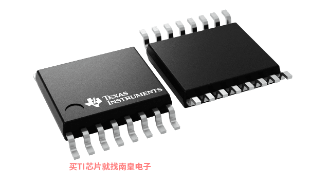
- Packaged in TSSOP
- Development and Programming Kit for Easy PLL Design and Programming (TI Pro-Clock)
- APPLICATIONS
- D-TVs, STBs, IP-STBs, DVD Players, DVD Recorders, and Printers
All other trademarks are the property of their respective owners
- Function
- Clock synthesizer
- Number of outputs
- 5
- Output frequency (Max) (MHz)
- 230
- Core supply voltage (V)
- 1.8
- Output supply voltage (V)
- 3.3, 2.5
- Input type
- XTAL, LVCMOS
- Output type
- LVCMOS
- Operating temperature range (C)
- -40 to 85
- Features
- Integrated EEPROM, Multiplier or divider, Spread-spectrum clocking (SSC)
- Rating
- Catalog
CDCE925的完整型号有:CDCE925PW、CDCE925PWR,以下是这些产品的关键参数及官网采购报价:
CDCE925PW,工作温度:-40 to 85,封装:TSSOP (PW)-16,包装数量MPQ:90个,MSL 等级/回流焊峰值温度:Level-1-260C-UNLIM,引脚镀层/焊球材料:NIPDAU,TI官网CDCE925PW的批量USD价格:2.038(1000+)
CDCE925PWR,工作温度:-40 to 85,封装:TSSOP (PW)-16,包装数量MPQ:2000个,MSL 等级/回流焊峰值温度:Level-1-260C-UNLIM,引脚镀层/焊球材料:NIPDAU,TI官网CDCE925PWR的批量USD价格:1.698(1000+)

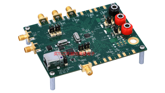
CDCE925PERF-EVM CDCE925 性能评估模块
The CDCE925Perf-Evaluation Module allows the verification of the functionality and performance of CDCE925 and CDCEL925 with the options of crystal and 1.8V LVCMOS inputs. The outputs can be connected to the Oscilloscope directly with SMA cables.
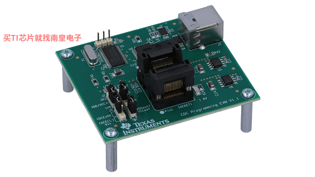
CDCEL9XXPROGEVM CDCE(L)949 系列 EEPROM 编程板
CDCE(L)949 系列时钟发生器集成了 EEPROM,允许在启动后保存默认频率设置。CDCEL9XXPROGEVM 是允许对原型样片或小批量生产进行快速编程的编程板。它适用于该系列的全部 8 款器件:CDCE949、CDCE937、CDCE925、CDCE913、CDCEL949、CDCEL937、CDCEL925 和 CDCEL913,并且带有易于使用的通用插座。
此外还提供另一个用于性能测试和评估的 EVM,其器件型号为 CDCE(L)9xxPERF-EVM,此性能评估模块适用于每个单独器件。
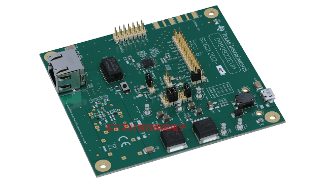
DP83822EVM DP83822I 10Mbps 和 100Mbps 以太网 PHY 评估模块
DP83822EVM 支持 100BASE-FX、100BASE-TX 和 10BASE-Te。此参考设计已通过 UNH 的合规性测试和验证。它还经过 A 级排放认证,符合 +/-8kV IEC61000-4-2(接触放电)标准。
DP83822EVM 包括两个板载状态 LED、带有板载 LDO 的 5V USB,并且可使用 USB-2-MDIO 工具进行 SMI 访问。提供 4 级搭接,因此无需直接访问 PHY 寄存器便可进行系统配置。外部电源可连接到各个指定电压轨以进行进一步系统评估。DP83822EVM 支持节能以太网、局域网唤醒、帧起始检测 IEEE 1588 时间戳和可配置 I/O (...)
CDCE925SW-LINUX 用于 CDCE925 的 Linux 驱动程序
Linux 驱动程序支持具有 2.5V 或 3.3V LVCMOS 输出的 CDCE925 可编程 2-PLL VCXO 时钟合成器。Linux 驱动程序支持通过 I2C 总线进行通信。Linux 主线状态
在 Linux 主线中提供:是
可通过 git.ti.com 获取:不适用
- cdce925
与该器件关联的文件为:
drivers/clk/clk-cdce925.c
Linux 器件树文档(...)
Drivers for the CDCEL9xx programmer EVM
TI's ClockPro software allows users to program/configure the following devices in a friendly GUI interface:- CDCE949
- CDCE937
- CDCE925
- CDCE913
- CDCE906
- CDCE706
- CDCEL949
- CDCEL937
- CDCEL925
- CDCEL913
It is intended to be used with the evaluation modules of the above devices.
ClockPro Software (Rev. E)
PSpice for TI 可提供帮助评估模拟电路功能的设计和仿真环境。此功能齐全的设计和仿真套件使用 Cadence 的模拟分析引擎。PSpice for TI 可免费使用,包括业内超大的模型库之一,涵盖我们的模拟和电源产品系列以及精选的模拟行为模型。借助PSpice for TI 的设计和仿真环境及其内置的模型库,您可对复杂的混合信号设计进行仿真。创建完整的终端设备设计和原型解决方案,然后再进行布局和制造,可缩短产品上市时间并降低开发成本。
在PSpice for TI 设计和仿真工具中,您可以搜索 TI (...)
CLOCK-TREE-ARCHITECT 时钟树架构编程软件
时钟树架构是一款时钟树综合工具,可根据您的系统要求生成时钟树解决方案,从而帮助您简化设计流程。该工具从庞大的时钟产品数据库中提取数据,然后生成系统级多芯片时钟解决方案。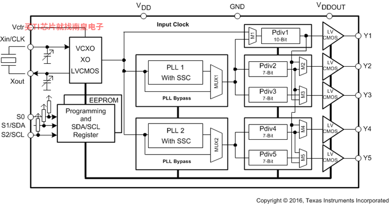
- MSP430FR5949
- AM26LV32E-EP
- REF3120
- TPS75225-EP
- ADS7829
- SN54ALS251
- TPS22918
- TLV2422
- TPS22986
- SN74ABTH18502A
- TDA3MA
- MC1489
- AM5K2E02
- TUSB213-Q1
- TXU0101
- UCC20225-Q1
- ISO6760L
- LP324-N
- THS3120
- MSP430FR6037
- TL494CNSR
- TPS76727QD
- LMX2330USLBX
- LM4040D25QDBZTG4
- LM2830XMFX/NOPB
- BQ20Z80DBTR
- SN761678BDBT
- DRV8881PRHRT
- TPS70148PWPR
- LM3813MX-7.0
- SNJ54AHCT14J
- O386050EDCARQ1
- UCC3957M-3G4
- TLV70734DQNR
- INA821IDGKR
- DAC3482IRKD25
- TLC1543QDBG4
- HPA01202BDKDR
- MSPM0G3107SDGS20R
- UA78M33CDCYR
