

- 制造厂商:TI(德州仪器,Texas Instruments)
- 产品类别:逻辑和电压转换
- 技术类目:电压转换器和电平转换器 - 方向控制型电压转换器
- 功能描述:具有可配置电压转换和三态输出的 2 位双电源总线收发器
- 点击这里打开及下载SN74LVC2T45的技术文档资料
- TI代理渠道,提供当日发货、严格的质量标准,满足您的目标价格

This dual-bit noninverting bus transceiver uses two separate configurable power-supply rails. The A port is designed to track VCCA. VCCA accepts any supply voltage from 1.65 V to 5.5 V. The B port is designed to track VCCB. VCCB accepts any supply voltage from 1.65 V to 5.5 V. This allows for universal low-voltage bidirectional translation between any of the 1.8-V, 2.5-V, 3.3-V, and 5-V voltage nodes.
The SN74LVC2T45 is designed for asynchronous communication between two data buses. The logic levels of the direction-control (DIR) input activate either the B-port outputs or the A-port outputs. The device transmits data from the A bus to the B bus when the B-port outputs are activated, and from the B bus to the A bus when the A-port outputs are activated. The input circuitry on both A and B ports are always active and must have a logic HIGH or LOW level applied to prevent excess ICC and ICCZ.
The SN74LVC2T45 is designed so that VCCA supplies the DIR input circuit. This device is fully specified for partial-power-down applications using Ioff. The Ioff circuitry disables the outputs, preventing damaging current backflow through the device when it is powered down.
The VCC isolation feature ensures that if either VCC input is at GND, both ports are in the high-impedance state.
- Fully configurable dual-rail design allows each port to operate over the full 1.65-V to 5.5-V power-supply range
- VCC isolation feature if either VCC input is at GND, both ports are in the high-impedance state
- DIR input circuit referenced to VCCA
- Low power consumption, 4-A maximum ICC
- Available in the Texas Instruments NanoFree package
- ±24-mA output drive at 3.3 V
- Ioff supports Partial-Power-Down mode operation
- Maximum data rates:
- 420 Mbps (3.3-V to 5-V translation)
- 210 Mbps (translate to 3.3 V)
- 140 Mbps (translate to 2.5 V)
- 75 Mbps (translate to 1.8 V)
- Latch-up performance exceeds 100 mA per JESD 78, Class II
- ESD protection exceeds JESD 22
- 4000-V Human-Body Model (A114-A)
- 200-V Machine Model (A115-A)
- 1000-V Charged-Device Model (C101)
- Technology Family
- LVC
- Applications
- GPIO, I2S
- Bits (#)
- 2
- High input voltage (Min) (Vih)
- 1.08
- High input voltage (Max) (Vih)
- 5.5
- Vout (Min) (V)
- 1.65
- Vout (Max) (V)
- 5.5
- IOH (Max) (mA)
- -32
- IOL (Max) (mA)
- 32
- Rating
- Catalog
SN74LVC2T45的完整型号有:SN74LVC2T45DCTR、SN74LVC2T45DCTT、SN74LVC2T45DCUR、SN74LVC2T45DCURG4、SN74LVC2T45DCUT、SN74LVC2T45DCUTG4、SN74LVC2T45YZPR,以下是这些产品的关键参数及官网采购报价:
SN74LVC2T45DCTR,工作温度:-40 to 85,封装:SM8 (DCT)-8,包装数量MPQ:3000个,MSL 等级/回流焊峰值温度:Level-1-260C-UNLIM,引脚镀层/焊球材料:NIPDAU,TI官网SN74LVC2T45DCTR的批量USD价格:.286(1000+)
SN74LVC2T45DCTT,工作温度:-40 to 85,封装:SM8 (DCT)-8,包装数量MPQ:250个,MSL 等级/回流焊峰值温度:Level-1-260C-UNLIM,引脚镀层/焊球材料:NIPDAU,TI官网SN74LVC2T45DCTT的批量USD价格:.443(1000+)
SN74LVC2T45DCUR,工作温度:-40 to 85,封装:VSSOP (DCU)-8,包装数量MPQ:3000个,MSL 等级/回流焊峰值温度:Level-1-260C-UNLIM,引脚镀层/焊球材料:NIPDAU,TI官网SN74LVC2T45DCUR的批量USD价格:.286(1000+)
SN74LVC2T45DCURG4,工作温度:-40 to 85,封装:VSSOP (DCU)-8,包装数量MPQ:3000个,MSL 等级/回流焊峰值温度:Level-1-260C-UNLIM,引脚镀层/焊球材料:NIPDAU,TI官网SN74LVC2T45DCURG4的批量USD价格:.329(1000+)
SN74LVC2T45DCUT,工作温度:-40 to 85,封装:VSSOP (DCU)-8,包装数量MPQ:250个,MSL 等级/回流焊峰值温度:Level-1-260C-UNLIM,引脚镀层/焊球材料:NIPDAU,TI官网SN74LVC2T45DCUT的批量USD价格:.343(1000+)
SN74LVC2T45DCUTG4,工作温度:-40 to 85,封装:VSSOP (DCU)-8,包装数量MPQ:250个,MSL 等级/回流焊峰值温度:Level-1-260C-UNLIM,引脚镀层/焊球材料:NIPDAU,TI官网SN74LVC2T45DCUTG4的批量USD价格:.386(1000+)
SN74LVC2T45YZPR,工作温度:-40 to 85,封装:DSBGA (YZP)-8,包装数量MPQ:3000个,MSL 等级/回流焊峰值温度:Level-1-260C-UNLIM,引脚镀层/焊球材料:SNAGCU,TI官网SN74LVC2T45YZPR的批量USD价格:.309(1000+)

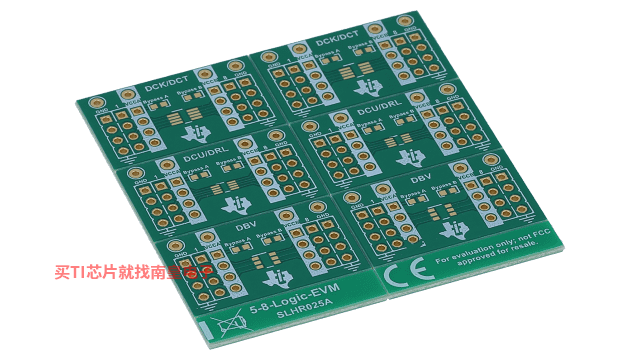
5-8-LOGIC-EVM 支持 5 至 8 引脚 DCK、DCT、DCU、DRL 和 DBV 封装的通用逻辑 EVM
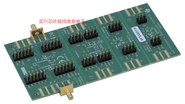
灵活的 EVM 设计用于支持具有 5 至 8 引脚数且采用 DCK、DCT、DCU、DRL 或 DBV 封装的任何器件。AVCLVCDIRCNTRL-EVM 适用于方向控制双向转换器件、支持 AVC 和 LVC 的通用 EVM
该通用 EVM 旨在支持 1、2、4 和 8 通道 LVC 和 AVC 方向控制转换器件。它还以相同数量的通道支持总线保持和汽车 Q1 器件。AVC 是低电压转换器件,具有 12mA 的较低驱动强度。LVC 是 1.65 至 5.5V 的较高电压转换器件,具有 32mA 的较高驱动强度。
SN74LVC2T45 IBIS Model (Rev. A)
该参考设计展示了 EnDat 2.2 编码器的稳定接口。这其中展示了 EMC 抗扰性,尤其是逆变器开关噪声等快速瞬变抗扰性。编码器电源电压是可配置的并集成了短路保护,以防止由于电缆短路或误接线而造成的损坏,还集成了诊断反馈以检测故障。此逻辑接口支持 3.3V 至 1.8V 的 IO。此设计采用 BoosterPack™ 开发套件,可利用 C2000™ MCU 轻松评估 EnDat2.2。该设计已针对几个 EnDat 2.2 编码器进行测试,适用的电缆长度最大为 100m。TIDA-01630 适用于 Tamagawa 编码器的高 EMC 抗扰度 RS485 接口参考设计
EMC immunity, especially immunity against inverter switching noise, is important for positioning encoder feedback systems of industrial drives. This design demonstrates a high EMC immunity RS485 transceiver solution which can be used on both the drive and encoder, such as Tamagawa™, EnDat (...)TIDA-01401 用于绝对编码器的高 EMC 抗扰度 RS-485 接口参考设计
该高 EMC 抗扰度参考设计展示了用于驱动器和编码器(如 EnDat 2.2、BiSS®、Tamagawa™ 等)的 RS-485 收发器。EMC 抗扰度(尤其是逆变器开关噪声抗扰度)对于工业驱动器中的位置编码器反馈系统而言非常重要。该设计支持 5 至 15V(标称值为 12V)宽输入电压范围(用作到编码器的输出电压),以满足编码器的宽电源范围要求。该设计的电源根据所选编码器的电压范围提供了过压和短路保护,以防电缆短路期间造成损坏。此设计包含具有与 TI LaunchPad™ 开发套件兼容的连接器的 BoosterPack™ 插件模块外形,可利用 (...)TIDM-ULTRASONIC-WATER-FLOW-MEASUREMENT 超声波水流测量参考设计
超声波水流测量系统非常适用于在低至 1.4 gpm 的宽流量范围中进行高精度的测量。该设计基于带分离的模拟组件的单个 MCU。它使用了一种独特的专有算法,该算法能改善很多种操作条件下的流量测量的稳健性和性能。该设计完全兼容用于无线 AMI 网络的 TI RF 插入式评估模块。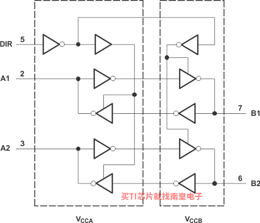
- LP5951
- SN74AHC1G08-Q1
- TPD6F202
- TPIC6273
- SN54ABT646A
- DS90CF364
- AM4378
- DAC53608
- TPS25832-Q1
- SN74LS221
- MSP430F5517
- DRV8962
- UC1825A-SP
- SN54AS821A
- DRV2700
- ADC141S628-Q1
- TL1431M
- DAC63002
- DLPC3439
- CSD17573Q5B
- TPS65941212RWERQ1
- TPS76725QDR
- SN74ALS243ANS
- CC1310F128RSMT
- TPS92510DGQ
- TRSF3223IPWRG4
- LM26CIM5-YPA
- DAC53608EVM
- TPS6503520HRZDRQ1
- TPS40425RHAR
- SN65LVDS305ZQE
- SM72240MFE-4.63/NOPB
- TMP708AIDBVT
- TPS65132B5YFFR
- LP3891EMRX-1.5/NOPB
- ADS1015IDGST
- INA149AMDREP
- SN74AS174NS
- LP38841MRX-ADJ
- UCC27201DR
