

- 制造厂商:TI(德州仪器,Texas Instruments)
- 产品类别:逻辑和电压转换
- 技术类目:触发器、锁存器和寄存器 - D 型触发器
- 功能描述:汽车类具有三态输出的八路边沿 D 类触发器
- 点击这里打开及下载SN74LVC574A-Q1的技术文档资料
- TI代理渠道,提供当日发货、严格的质量标准,满足您的目标价格

The SN74LVC574A octal edge-triggered D-type flip-flop is designed for 2.7-V to 3.6-V VCC operation.
This device features 3-state outputs designed specifically for driving highly capacitive or relatively low-impedance loads. It is particularly suitable for implementing buffer registers, I/O ports, bidirectional bus drivers, and working registers.
On the positive transition of the clock (CLK) input, the Q outputs are set to the logic levels at the data (D) inputs.
A buffered output-enable (OE) input can be used to place the eight outputs in either a normal logic state (high or low logic levels) or the high-impedance state. In the high-impedance state, the outputs neither load nor drive the bus lines significantly. The high-impedance state and increased drive provide the capability to drive bus lines without interface or pullup components.
OE does not affect the internal operations of the flip-flops. Old data can be retained or new data can be entered while the outputs are in the high-impedance state.
This device is fully specified for partial-power-down applications using Ioff. The Ioff circuitry disables the outputs, preventing damaging current backflow through the device when it is powered down.
To ensure the high-impedance state during power up or power down, OE should be tied to VCC through a pullup resistor; the minimum value of the resistor is determined by the current-sinking capability of the driver.
Inputs can be driven from either 3.3-V or 5-V devices. This feature allows the use of thIs device as a translator in a mixed 3.3-V/5-V system environment.
- Qualified for Automotive Applications
- ESD Protection Exceeds 2000 V Per MIL-STD-883, Method 3015; Exceeds 200 V Using Machine Model (C = 200 pF, R = 0)
- Operates From 2 V to 3.6 V
- Inputs Accept Voltages to 5.5 V
- Max tpd of 7 ns at 3.3 V
- Typical VOLP (Output Ground Bounce) < 0.8 V at VCC = 3.3 V, TA = 25°C
- Typical VOHV (Output VOH Undershoot) > 2 V at VCC = 3.3 V, TA = 25°C
- Supports Mixed-Mode Signal Operation on All Ports (5-V Input/Output Voltage With 3.3-V VCC)
- Ioff Supports Partial-Power-Down Mode Operation
- Number of channels (#)
- 8
- Technology Family
- LVC
- Supply voltage (Min) (V)
- 2
- Supply voltage (Max) (V)
- 3.6
- Input type
- Standard CMOS
- Output type
- 3-State
- Clock Frequency (Max) (MHz)
- 100
- IOL (Max) (mA)
- 24
- IOH (Max) (mA)
- -24
- ICC (Max) (uA)
- 10
- Features
- Balanced outputs, Very high speed (tpd 5-10ns), Over-voltage tolerant inputs, Partial power down (Ioff)
SN74LVC574A-Q1的完整型号有:CLVC574AQDWRG4Q1、CLVC574AQPWRG4Q1、SN74LVC574AQDWRQ1,以下是这些产品的关键参数及官网采购报价:
CLVC574AQDWRG4Q1,工作温度:-40 to 125,封装:SOIC (DW)-20,包装数量MPQ:2000个,MSL 等级/回流焊峰值温度:Level-1-260C-UNLIM,引脚镀层/焊球材料:NIPDAU,TI官网CLVC574AQDWRG4Q1的批量USD价格:.307(1000+)
CLVC574AQPWRG4Q1,工作温度:-40 to 125,封装:TSSOP (PW)-20,包装数量MPQ:2000个,MSL 等级/回流焊峰值温度:Level-1-260C-UNLIM,引脚镀层/焊球材料:NIPDAU,TI官网CLVC574AQPWRG4Q1的批量USD价格:.307(1000+)
SN74LVC574AQDWRQ1,工作温度:-40 to 125,封装:SOIC (DW)-20,包装数量MPQ:2000个,MSL 等级/回流焊峰值温度:Level-1-260C-UNLIM,引脚镀层/焊球材料:NIPDAU,TI官网SN74LVC574AQDWRQ1的批量USD价格:.272(1000+)

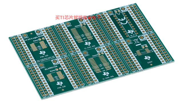
14-24-LOGIC-EVM 支持 14 到 24 引脚 PW、DB、D、DW、NS、DYY 和 DGV 封装的通用逻辑 EVM
该 EVM 设计用于支持采用 14 至 24 引脚 D、DW、DB、NS、PW、DYY 或 DGV 封装的任何逻辑器件。
- LM43600-Q1
- TLV2432
- TPS43350-Q1
- SN54LS02
- CD4052B-MIL
- TPS22860
- TPS2300
- THS4082
- SN75462
- LMS33460
- LM7332
- TPS3820
- CD54HC173
- UCC5870-Q1
- CD4044B-MIL
- MSP430F6459
- SN74ALS244C-1
- LMV842-Q1
- CSD19534Q5A
- LP87562-Q1
- SN74GTLPH16612DLR
- LM2937ESX-2.5/NOPB
- TLE2022AQDRQ1
- UCC38085PW
- THS3122CDDAR
- SN74AS874NT
- ISO7840FDWR
- LM4050BEM3X-2.5
- UC3825N
- CD4071BPWE4
- LMV824IPWR
- SN74LVC2952ADW
- REF7012QDGKR
- OPA2380AIDGKRG4
- TPS60400DBVRG4
- LP3982ILDX-1.8
- DS90UH929TRGCTQ1
- CD74HCT4020M96
- SN74HCT374DBR
- TPS2513EVM-527
