
- 制造厂商:TI(德州仪器,Texas Instruments)
- 产品类别:逻辑和电压转换
- 技术类目:缓冲器、驱动器和收发器 - 反向缓冲器和驱动器
- 功能描述:具有三态输出的 2 通道、1.65V 至 5.5V 反相器
- 点击这里打开及下载SN74LVC2G240的技术文档资料
- TI代理渠道,提供当日发货、严格的质量标准,满足您的目标价格

This dual buffer driver is designed for 1.65-V to 5.5-V VCC operation.
The SN74LVC2G240 device is designed specifically to improve the performance and density of 3-state memory address drivers, clock drivers, and bus-oriented receivers and transmitters.
NanoFree™ package technology is a major breakthrough in IC packaging concepts, using the die as the package.
This device is organized as two 1-bit buffers/drivers with separate output-enable (OE) inputs. When OE is low, the device passes data from the A input to the Y output. When OE is high, the outputs are in the high-impedance state.
To ensure the high-impedance state during power up or power down, OE should be tied to VCC through a pullup resistor; the minimum value of the resistor is determined by the current-sinking capability of the driver.
This device is fully specified for partial-power-down applications using Ioff. The Ioff circuitry disables the outputs, preventing damaging current backflow through the device when it is powered down.
- Available in the Texas Instruments NanoFree Package
- Supports 5-V VCC Operation
- Inputs Accept Voltages to 5.5 V
- Max tpd of 4.6 ns at 3.3 V
- Low Power Consumption, 10-A Max ICC
- ±24-mA Output Drive at 3.3 V
- Typical VOLP (Output Ground Bounce) <0.8 V at VCC = 3.3 V, TA = 25°C
- Typical VOHV (Output VOH Undershoot) >2 V at VCC = 3.3 V, TA = 25°C
- Ioff Supports Live Insertion, Partial-Power-Down Mode, and Back-Drive Protection
- Can Be Used as a Down Translator to Translate Inputs From a Max of 5.5 V Down to the VCC Level
- Latch-Up Performance Exceeds 100 mA Per JESD 78, Class II
- ESD Protection Exceeds JESD 22
- 2000-V Human-Body Model (A114-A)
- 1000-V Charged-Device Model (C101)
- Technology Family
- LVC
- Supply voltage (Min) (V)
- 1.65
- Supply voltage (Max) (V)
- 5.5
- Number of channels (#)
- 2
- IOL (Max) (mA)
- 32
- IOH (Max) (mA)
- -32
- ICC (Max) (uA)
- 10
- Input type
- Standard CMOS
- Output type
- 3-State
- Features
- Balanced outputs, Very high speed (tpd 5-10ns), Partial power down (Ioff), Over-voltage tolerant inputs
- Rating
- Catalog
SN74LVC2G240的完整型号有:74LVC2G240DCURG4、SN74LVC2G240DCTR、SN74LVC2G240DCUR、SN74LVC2G240YZPR,以下是这些产品的关键参数及官网采购报价:
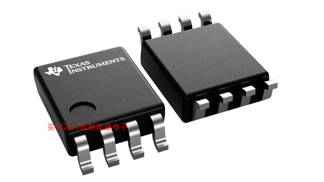
74LVC2G240DCURG4,工作温度:-40 to 125,封装:VSSOP (DCU)-8,包装数量MPQ:3000个,MSL 等级/回流焊峰值温度:Level-1-260C-UNLIM,引脚镀层/焊球材料:NIPDAU,TI官网74LVC2G240DCURG4的批量USD价格:.205(1000+)
SN74LVC2G240DCTR,工作温度:-40 to 125,封装:SM8 (DCT)-8,包装数量MPQ:3000个,MSL 等级/回流焊峰值温度:Level-1-260C-UNLIM,引脚镀层/焊球材料:NIPDAU,TI官网SN74LVC2G240DCTR的批量USD价格:.223(1000+)
SN74LVC2G240DCUR,工作温度:-40 to 125,封装:VSSOP (DCU)-8,包装数量MPQ:3000个,MSL 等级/回流焊峰值温度:Level-1-260C-UNLIM,引脚镀层/焊球材料:SN,TI官网SN74LVC2G240DCUR的批量USD价格:.15(1000+)
SN74LVC2G240YZPR,工作温度:-40 to 125,封装:DSBGA (YZP)-8,包装数量MPQ:3000个,MSL 等级/回流焊峰值温度:Level-1-260C-UNLIM,引脚镀层/焊球材料:SNAGCU,TI官网SN74LVC2G240YZPR的批量USD价格:.238(1000+)

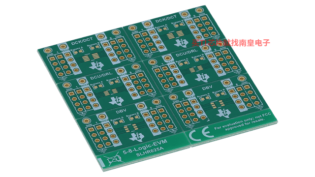
5-8-LOGIC-EVM 支持 5 至 8 引脚 DCK、DCT、DCU、DRL 和 DBV 封装的通用逻辑 EVM
灵活的 EVM 设计用于支持具有 5 至 8 引脚数且采用 DCK、DCT、DCU、DRL 或 DBV 封装的任何器件。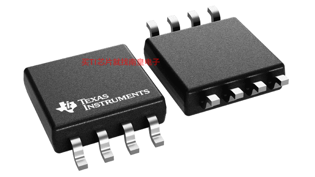
- TPS65084
- SN74LVC1G32
- SN65HVD30-EP
- TPS40192
- TPS826765
- TL081H
- TS5A23157
- TPS2812
- TPS560200-Q1
- TS5A3157
- MSP430FR59721
- CD54HCT390
- TPS92010
- MSP430F2132-EP
- TLV2444
- MAX3237E
- SN65HVD1792-EP
- SN74VMEH22501
- TCA9543A
- SN74AXC4T774-Q1
- MDL-BDC-B
- PT5504N
- SN74ALS244C-1N
- CD4517BE
- TLE2144MDWREP
- TPS3430WDRCR
- 76002012A
- LME49870MA/NOPB
- LM65645SRZTRQ1
- DAC8565IBPWRG4
- SN74CBT16211DLR
- LM25116MHX
- TPS65835EVM-705
- SNJ5416J
- TL431BCLPR
- TPS65632AGRTER
- TLA2022IRUGR
- OPA2322AIDGKR
- LMV111M7
- SN74ACT3638-20PCB
