

- жЦдьГЇЩЬЃКTIЃЈЕТжнвЧЦїЃЌTexas InstrumentsЃЉ
- ВњЦЗРрБ№ЃКЪ§ОнзЊЛЛЦї
- ММЪѕРрФПЃКФЃЪ§зЊЛЛЦї (ADC) - ИпЫйФЃЪ§зЊЛЛЦї (>10MSPS)
- ЙІФмУшЪіЃК10 ЮЛ 40MSPS Ъ§ФЃзЊЛЛЦї (ADC) - ЗћКЯЦћГЕгІгУБъзМ
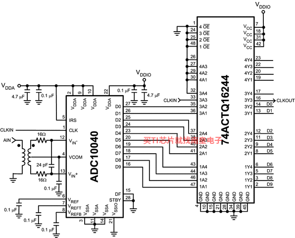
- ЕуЛїетРяДђПЊМАЯТдиADC10040-Q1ЕФММЪѕЮФЕЕзЪСЯ
- TIДњРэЧўЕРЃЌЬсЙЉЕБШеЗЂЛѕЁЂбЯИёЕФжЪСПБъзМЃЌТњзуФњЕФФПБъМлИё

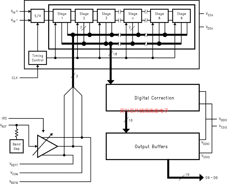
The ADC10040 is a monolithic CMOS analog-to-digital converter capable of converting analog input signals into 10-bit digital words at 40 Megasamples per second (MSPS). This converter uses a differential, pipeline architecture with digital error correction and an on-chip sample-and-hold circuit to provide a complete conversion solution, and to minimize power consumption, while providing excellent dynamic performance. A unique sample-and-hold stage yields a full-power bandwidth of 400 MHz. Operating on a single 3.0V power supply, this device consumes just 55.5 mW at 40 MSPS, including the reference current. The Standby feature reduces power consumption to just 13.5 mW.
The differential inputs provide a full scale selectable input swing of 2.0 VP-P, 1.5 VP-P, 1.0 VP-P, with the possibility of a single-ended input. Full use of the differential input is recommended for optimum performance. An internal +1.2V precision bandgap reference is used to set the ADC full-scale range, and also allows the user to supply a buffered referenced voltage for those applications requiring increased accuracy. The output data format is user choice of offset binary or two’s complement.
The ADC10040Q runs on an Automotive Grade Flow and is AEC-Q100 Grade 3 Qualified.
This device is available in the 28-lead TSSOP package and will operate over the industrial temperature range of −40°C to +85°C.
- Single +3.0V Operation
- Selectable 2.0 VP-P, 1.5 VP-P, or 1.0 VP-P full-scale input swing
- 400 MHz 3 dB Input Bandwidth
- Low Power Consumption
- Standby Mode
- On-Chip Reference and Sample-and-Hold Amplifier
- Offset Binary or TwoЁЏs Complement Data Format
- Separate Adjustable Output Driver Supply to Accommodate 2.5V and 3.3V Logic Families
- AEC-Q100 Grade 3 Qualified
- 28-Pin TSSOP Package
- Resolution: 10 Bits
- Conversion Rate: 40 MSPS
- Full Power Bandwidth: 400 MHz
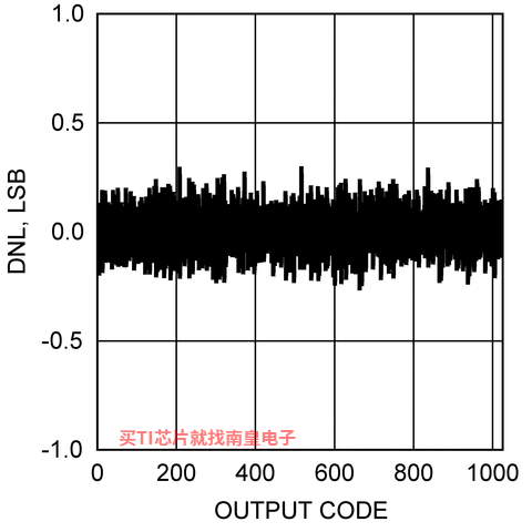
- DNL: ЁР0.3 LSB typ)
- SNR (fIN = 11 MHz): 59.6 dB (typ)
- SFDR (fIN = 11 MHz): -80 dB (typ)
- Power Consumption, 40 MHz: 55.5 mW
All trademarks are the property of their respective owners.
- Sample rate (Max) (MSPS)
- 40
- Resolution (Bits)
- 10
- Number of input channels
- 1
- Interface type
- Parallel CMOS, TTL
- Analog input BW (MHz)
- 400
- Features
- Low Power
- Rating
- Automotive
- Input range (Vp-p)
- 2
- Power consumption (Typ) (mW)
- 55.5
- Architecture
- Pipeline
- SNR (dB)
- 58.7
- ENOB (Bits)
- 9.6
- SFDR (dB)
- 80
- Operating temperature range (C)
- -40 to 85
- Input buffer
- No
ADC10040-Q1ЕФЭъећаЭКХгаЃКADC10040QCIMT/NOPBЁЂADC10040QCIMTX/NOPBЃЌвдЯТЪЧетаЉВњЦЗЕФЙиМќВЮЪ§МАЙйЭјВЩЙКБЈМлЃК
ADC10040QCIMT/NOPBЃЌЙЄзїЮТЖШЃК-40 to 85ЃЌЗтзАЃКTSSOP (PW)-28ЃЌАќзАЪ§СПMPQЃК48ИіЃЌMSL ЕШМЖ/ЛиСїКИЗхжЕЮТЖШЃКLevel-3-260C-168 HRЃЌв§НХЖЦВу/КИЧђВФСЯЃКSNЃЌTIЙйЭјADC10040QCIMT/NOPBЕФХњСПUSDМлИёЃК4.974ЃЈ1000+ЃЉ
ADC10040QCIMTX/NOPBЃЌЙЄзїЮТЖШЃК-40 to 85ЃЌЗтзАЃКTSSOP (PW)-28ЃЌАќзАЪ§СПMPQЃК2500ИіЃЌMSL ЕШМЖ/ЛиСїКИЗхжЕЮТЖШЃКLevel-3-260C-168 HRЃЌв§НХЖЦВу/КИЧђВФСЯЃКSNЃЌTIЙйЭјADC10040QCIMTX/NOPBЕФХњСПUSDМлИёЃК4.253ЃЈ1000+ЃЉ

PSPICE-FOR-TI ЪЪгУгк TI ЩшМЦКЭФЃФтЙЄОпЕФ PSpice
PSpice for TI ПЩЬсЙЉАяжњЦРЙРФЃФтЕчТЗЙІФмЕФЩшМЦКЭЗТецЛЗОГЁЃДЫЙІФмЦыШЋЕФЩшМЦКЭЗТецЬзМўЪЙгУ Cadence ЕФФЃФтЗжЮів§ЧцЁЃPSpice for TI ПЩУтЗбЪЙгУЃЌАќРЈвЕФкГЌДѓЕФФЃаЭПтжЎвЛЃЌКИЧЮвУЧЕФФЃФтКЭЕчдДВњЦЗЯЕСавдМАОЋбЁЕФФЃФтааЮЊФЃаЭЁЃНшжњPSpice for TI ЕФЩшМЦКЭЗТецЛЗОГМАЦфФкжУЕФФЃаЭПтЃЌФњПЩЖдИДдгЕФЛьКЯаХКХЩшМЦНјааЗТецЁЃДДНЈЭъећЕФжеЖЫЩшБИЩшМЦКЭдаЭНтОіЗНАИЃЌШЛКѓдйНјааВМОжКЭжЦдьЃЌПЩЫѕЖЬВњЦЗЩЯЪаЪБМфВЂНЕЕЭПЊЗЂГЩБОЁЃ
дкPSpice for TI ЩшМЦКЭЗТецЙЄОпжаЃЌФњПЩвдЫбЫї TI (...)
- ADS62PF49
- TL16C750E
- LMC6001
- TLV9104
- UC3842M
- INA271A-Q1
- MSP430F4260
- LMR16006
- CD54ACT574
- TPS563231
- TS3A5223
- THVD1449V
- ADS8341
- LP2996-N
- TPS54JB20
- ONET8501V
- TAS5722L
- SN74ABTH16245
- UCC20225-Q1
- SN74LVC257A-Q1
- LP38841SX-1.5/NOPB
- TLE2022CPG4
- TPS728175295YZUR
- RM46L440CPGET
- LMX25412060EVAL/NOPB
- SN74ALS870NT
- CD74HC4060PW
- ONET4211LDRGET
- RES21A90QDDFRQ1
- LM2917M
- INA2332AIPWT
- DS8921N/NOPB
- SN74LVTH241NSR
- TPS78101DRVT
- DRV8320RHRHAT
- THS4511RGTRG4
- SN74HCT08PW
- XAM1707BZKB4
- TPS563203EVM
- LMZ12001TZE-ADJ/NOPB
